The expansion of 5G networks is transforming the global communication landscape, bringing faster speeds, lower latency, and the ability to connect more devices than ever before. At the core of this technological revolution lies a critical component: the HDI printed circuit board (PCB). High-Density Interconnector (HDI) PCBs are playing a pivotal role in enabling the high-speed, high-efficiency, and miniaturization requirements that 5G infrastructure demands. This article delves into how HDI PCBs are integral to the development and deployment of 5G networks.
Understanding HDI Printed Circuit Boards
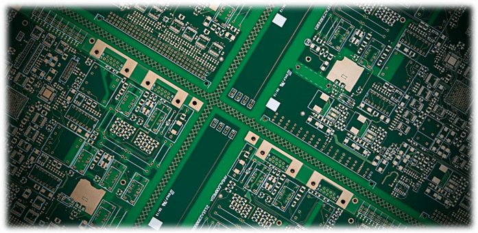
Before we dive into the role of HDI in 5G expansion, it’s essential to understand what HDI PCBs are. HDI PCBs are advanced circuit boards designed with a higher density of electronic components and connections compared to traditional PCBs. These boards are characterized by smaller traces and vias, and they often feature micro-vias and blind vias. The enhanced density and reduced size of HDI PCBs make them ideal for modern electronic devices, especially those requiring higher processing power and connectivity.
The growing demand for faster communication and more reliable connections in 5G networks has made HDI PCBs a critical component. As 5G technology requires small, efficient, and highly functional components, HDI PCBs are the perfect solution for meeting these demands.
The Role of HDI PCBs in 5G Network Expansion
The advent of 5G networks comes with unique challenges. The push for faster data transfer rates, reduced latency, and improved connectivity puts a strain on the design and production of communication devices and infrastructure. HDI PCBs address many of these challenges, and their role in the expansion of 5G networks is multifaceted.
Supporting High-Density Components
One of the primary benefits of HDI PCBs in 5G networks is their ability to accommodate high-density components. 5G systems require advanced components that need to be interconnected in smaller spaces. HDI PCBs are engineered to fit more components into a smaller area, which is essential for devices like 5G antennas, small cell networks, and edge computing nodes. This is crucial in the development of compact, high-performance 5G infrastructure.
To understand the importance of HDI PCBs in supporting high-density components, check over here how these boards allow for the integration of advanced technologies in a more space-efficient manner. Without HDI PCBs, it would be challenging to create the miniaturized devices that 5G requires, leading to larger, bulkier infrastructure that would hinder the network’s performance.
Minimizing Signal Loss and Interference
In the context of 5G, signal integrity is a key concern. 5G requires ultra-fast data transmission with minimal latency, meaning that any signal loss or interference can result in slower speeds and degraded network performance. HDI PCBs help to mitigate this by providing high-quality electrical performance with minimal signal loss. This is achieved by using micro-vias and fine traces that improve the conductivity and reduce the path length between components, allowing for faster data transfer.
The smaller vias and traces in HDI PCBs also reduce the amount of electromagnetic interference (EMI), which is crucial in the dense, high-frequency environments that 5G operates in. The quality of the signal can be maintained over longer distances, ensuring that 5G systems operate smoothly and without disruption.
Enabling Smaller, More Efficient Devices
With 5G technology, the demand for smaller and more efficient devices is greater than ever before. Traditional PCBs would struggle to meet these demands due to their larger size and less efficient use of space. HDI PCBs, on the other hand, are designed to maximize space utilization while maintaining the necessary connectivity and performance. This makes them ideal for 5G devices, where size is often a limiting factor.
HDI PCBs enable the development of smaller devices like smartphones, IoT devices, and wearable technologies that are essential for the growth of the 5G ecosystem. These boards help make these devices more powerful without increasing their size, allowing manufacturers to offer compact, portable, and efficient 5G-enabled products.
Improving Reliability and Durability
5G networks will be deployed in a variety of environments, from urban centers to rural areas, and even in harsh industrial settings. This means that the devices and infrastructure supporting the 5G network must be highly reliable and durable. HDI PCBs are known for their robustness, as they can withstand high temperatures, moisture, and physical stress.
By using HDI PCBs in 5G devices, manufacturers can ensure that the products will perform well in diverse conditions without failure. This durability is especially important in small cell networks, base stations, and remote sensing applications that will be integral to the success of 5G.
Supporting Advanced Features and Connectivity
5G technology promises to enable a host of new applications, from autonomous vehicles to smart cities and industrial IoT. To support these advanced features, 5G devices require high-speed data processing, extensive connectivity options, and the ability to handle complex tasks. HDI PCBs enable these capabilities by supporting high-speed signal transmission and providing the necessary connections between components.
These boards also support advanced features like beamforming and multiple-input multiple-output (MIMO) technology, which are crucial for optimizing the performance of 5G networks. By allowing for the integration of these complex features in a compact design, HDI PCBs contribute significantly to the capabilities of 5G infrastructure.
The Future of HDI PCBs in 5G Network Expansion
As 5G networks continue to grow, the demand for HDI PCBs will only increase. The future of 5G depends on the continuous improvement of electronic components that can meet the challenges of speed, size, and efficiency. HDI PCBs will remain at the forefront of this evolution, enabling the miniaturization and enhancement of the devices and infrastructure that will support next-generation networks.
To keep up with the pace of 5G deployment, manufacturers must continually innovate and improve their HDI PCB designs. This includes exploring new materials, improving signal integrity, and further reducing the size and cost of HDI PCBs.
Conclusion
HDI printed circuit boards are a cornerstone of the 5G revolution. Their ability to support high-density components, minimize signal loss, enable smaller devices, improve reliability, and support advanced features makes them indispensable in the expansion of 5G networks. As the demand for faster, more reliable, and more compact devices grows, HDI PCBs will continue to play a critical role in shaping the future of telecommunications.
For manufacturers and engineers looking to stay ahead of the curve in 5G technology, understanding the importance of HDI printed circuit boards is key. By leveraging the benefits of HDI PCBs, the full potential of 5G networks can be realized, enabling new innovations and opportunities in a highly connected world.